 Threads

In the fast-paced world of semiconductor manufacturing, keeping up with the latest technological advancements is crucial. Innovation in this field is greatly related to the concept of process nodes. In this article, I will discuss the world of process nodes, their significance, evolution, and the latest developments in this technology.
Key Takeaways
- Process nodes are the size of the transistor on a semiconductor chip.
- Each new node offers improved performance, reduced power consumption, and increased capabilities.
- Latest advancements include 3nm transitioning to 2nm and 1.4nm.
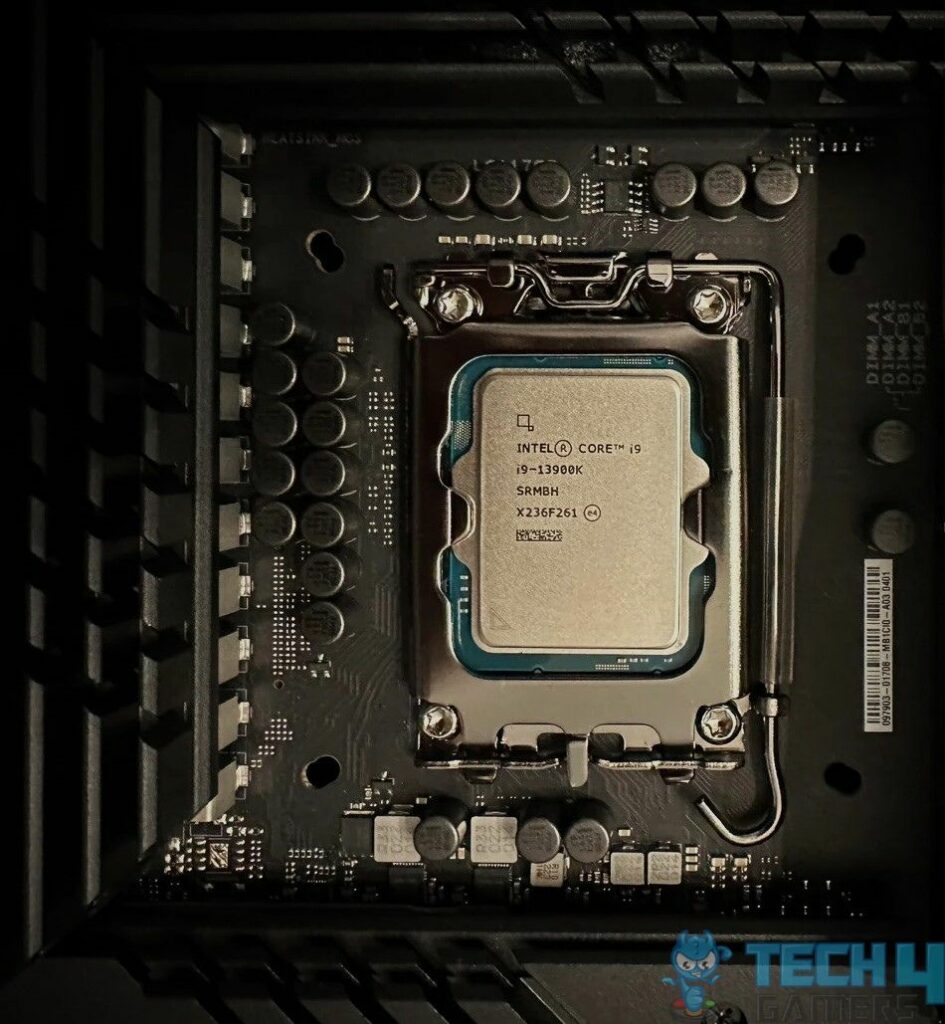
What Are Process Nodes?
Process nodes refer to the size of transistors and other components on a semiconductor chip. The term “node” is used to represent the technology’s generation and defines the size of the transistors, interconnects, and other features on the chip [1].
Evolution Of Process Nodes
Here is the crucial data I have gathered for the evolution of nodes from 1999 to 2024:
| Process Node | Year | Key Advancements and Applications |
|---|---|---|
| 180nm | 1999 | Advancements in mobile and early digital devices. |
| 130nm | 2000 | Improved transistor size and power efficiency. |
| 90nm | 2002 | Enhanced features and battery life for mobile devices. |
| 65nm | 2005 | Smaller, more efficient transistors, early smartphones. |
| 45nm | 2007 | Faster, power-efficient chips for mobile and computing. |
| 32nm | 2010 | Miniaturization, growth in mobile computing. |
| 22nm | 2012 | Introduction of 3D tri-gate transistors. |
| 14nm | 2014 | Improved transistor density and energy efficiency. |
| 10nm | 2017 | Smaller transistors for energy-efficient mobile devices. |
| 7nm | 2018 | High-performance processors, 5G technology, AI. |
| 5nm | 2020 | Powerful and energy-efficient chips for smartphones, AI. |
| 4nm | 2021 | Increased efficiency and performance |
| 3nm | 2022 | The 3nm process by TSMC stands out as the most cutting-edge semiconductor technology in the industry, providing optimal power, performance, and area (PPA). |
| 2nm | 2024 | TSMC plans to release it by the end of 2024 |
What Are The Latest Process Nodes?
As of 2024, the semiconductor industry is on the verge of transitioning to the 2nm process node. Here’s a glimpse of what I found in the world of 2nm process nodes:
- TSMC plans to begin production of a 2nm node in late 2024, with mass production following after[2].
- Intel also expects production in 2024[3].
- Samsung is aiming for 2nm mass production in 2025[4].
Looking Beyond 2nm
Samsung set ambitious goals, including mass-producing 1.4nm nodes by 2027, showcasing its commitment to pushing the boundaries of semiconductor technology[5].
Related helpful sources by Tech4Gamers:
References:
- Bharat Jha (Aachen University. The Evolution of Semiconductor Nodes. Retrieved from: https://www.linkedin.com/pulse/evolution-semiconductor-nodes-journey-innovation-progress-bharat-jha/
- TSMC. Future R&D Plans. Retrieved from: https://www.tsmc.com/english/dedicatedFoundry/technology/future_rd
- Intel Technology Roadmaps and Milestones. Retrieved from: https://www.intel.com/content/www/us/en/newsroom/news/intel-technology-roadmaps-milestones.html#gs.771oei
- Samsung News Room. Foundry Innovations Power the Future of Big Data. Retrieved from: https://news.samsung.com/global/samsung-foundry-innovations-power-the-future-of-big-data-ai-ml-and-smart-connected-devices
- Samsung News Room. Samsung Electronics Unveils Plans for 1.4nm Process Technology. Retrieved from: https://news.samsung.com/global/samsung-electronics-unveils-plans-for-1-4nm-process-technology-and-investment-for-production-capacity-at-samsung-foundry-forum-2022
FAQs
Process nodes determine the size and characteristics of components on semiconductor chips, which in turn affect a chip’s performance, power efficiency, and capabilities.
Transitioning to the 2nm process node brings increased transistor density, faster processing speeds, and reduced power consumption.
Scaling semiconductor technology beyond 3nm presents technical challenges related to power leakage and heat dissipation.
Thank you! Please share your positive feedback. 🔋
How could we improve this post? Please Help us. 😔
[Wiki Editor]
Ali Rashid Khan is an avid gamer, hardware enthusiast, photographer, and devoted litterateur with a period of experience spanning more than 14 years. Sporting a specialization with regards to the latest tech in flagship phones, gaming laptops, and top-of-the-line PCs, Ali is known for consistently presenting the most detailed objective perspective on all types of gaming products, ranging from the Best Motherboards, CPU Coolers, RAM kits, GPUs, and PSUs amongst numerous other peripherals. When he’s not busy writing, you’ll find Ali meddling with mechanical keyboards, indulging in vehicular racing, or professionally competing worldwide with fellow mind-sport athletes in Scrabble. Currently speaking, Ali’s about to complete his Bachelor’s in Business Administration from Bahria University Karachi Campus.
Get In Touch: alirashid@tech4gamers.com


